Failing to hack an IKEA smart remote
Recently I bought an IKEA smart remote mostly because I wanted to hack it. It costs less than 8 EUR, has a nice scroll wheel, and looked like the kind of device that might have interesting debug pads inside.
My original goal was simple: dump the firmware and, if I got lucky, run some of my own code on it.
The exact model is the IKEA BILRESA smart remote with a scroll wheel.
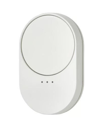
After some searching online, I found that it uses a Qorvo chip. More specifically, the module is based on the Qorvo QPG6200L, a wireless SoC that supports Matter over Thread, Zigbee, and Bluetooth Low Energy.
So I downloaded the chip datasheet, opened the remote, and started looking around.
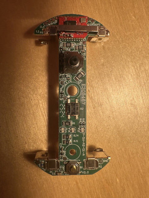
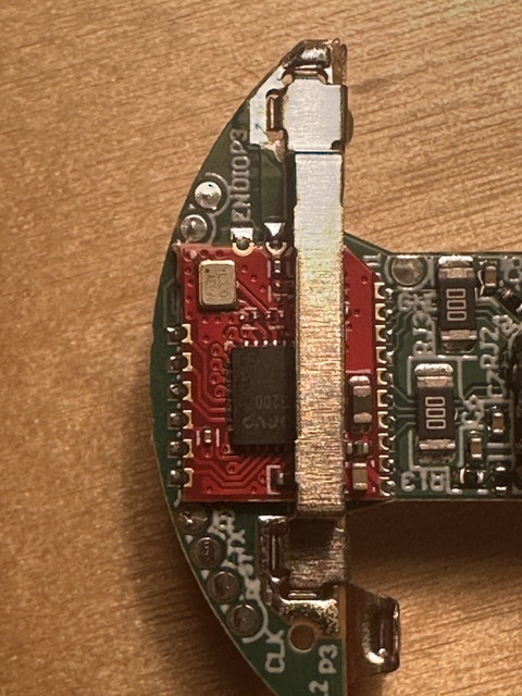
The SoC is on a small red module soldered onto the main PCB. On the top of the main board there are six very interesting pads:
- CLK
- RE ST
- TX
- RX
- ENDIO
- P3
TX and RX looked like UART, so that was the first thing to try. I soldered jumpers to TX, RX, and a ground pad on the bottom of the PCB, then connected them to my BRUSCHETTA-Board, which I usually use as a USB-UART adapter.
At 115200 baud, the device printed this on boot:
OTA header pointer is NULL.
Secure boot Enabled
Primary region
That is not much, but it is already useful:
OTA header pointer is NULL.probably means there is no staged OTA image.Secure boot Enabledmeans the ROM will not execute unsigned firmware.Primary regionmeans it is booting the primary application slot.
I tried sending input over UART, but I did not find an interactive shell or bootloader menu. So the next target was the other pads.
Finding the debug pins
At first glance, the remaining pads looked like debug/programming pins. CLK looked like a clock, RE ST was obviously reset, and ENDIO looked suspiciously like SWDIO.
I took a close-up photo of the module, traced the connections, and checked continuity from the module pins to the pads on the main PCB.
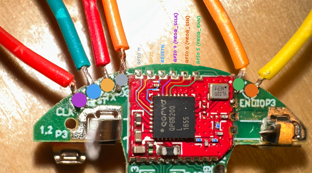
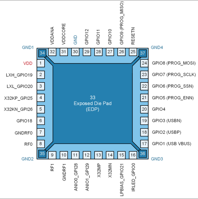
The useful pinout ended up being:
| Pad label | Chip pin | Programming mode | Debug mode |
|---|---|---|---|
| CLK | GPIO7 | PROG_SCLK | SWCLK / TCK |
| RE ST | RESETN | reset | reset |
| TX | GPIO10 | UART TX | UART TX |
| RX | GPIO11 | UART RX | UART RX |
| ENDIO | GPIO6 | PROG_ENN | debug enable strap |
| P3 | GPIO5 | PROG_SSN | SWDIO / TMS |
This is where the datasheet mattered. The same pins can be used for SPI programming or for SWD/JTAG debug, depending on the state of PROG_ENN during reset.
So my first guess was only half right. CLK really was the SWD clock, but ENDIO was not SWDIO. It was the strap used to select debug/programming mode. The actual SWDIO pad was P3.
To enter debug mode, the QPG6200L datasheet says to hold PROG_ENN low during reset, keep it low for about one second, then release it. On this board, PROG_ENN is the pad labeled ENDIO.
If you keep ENDIO low forever, the chip enters SPI programming mode instead. That is not what I wanted, and the full SPI programming interface was not available on this header anyway because MOSI and MISO were missing.
First wrong turn: the BRUSCHETTA board
My first attempt was to use the BRUSCHETTA-Board for SWD too. It uses a CH347, and recent OpenOCD has a ch347 adapter driver, so it looked promising.
It was not.
The board I have contains CH347T chip version 2.41. OpenOCD's CH347 SWD support requires newer silicon, so SWD initialization failed. JTAG mode was available, but the required JTAG data pins were not exposed on the IKEA header.
So the BRUSCHETTA stayed useful for UART, but not for SWD.
Second attempt: Pico debugprobe
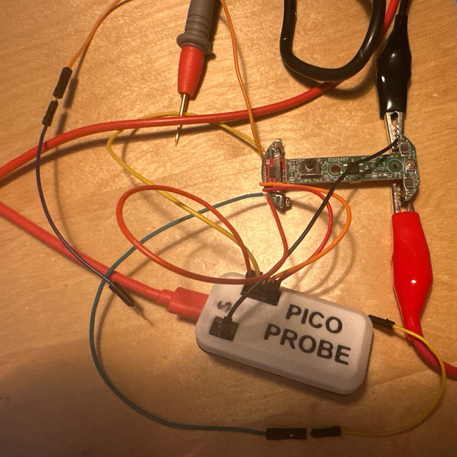
I flashed a Raspberry Pi Pico with the debugprobe firmware and wired it like this:
| Pico debugprobe | IKEA board |
|---|---|
| GP2 / SWCLK | CLK |
| GP3 / SWDIO | P3 |
| GND | GND |
The Pico was USB-powered. I left the IKEA remote powered from its own batteries and only connected the grounds together. Do not feed 5 V into this board.
Before this project I had basically no experience with OpenOCD or SWD, so I used an AI agent to help me build an OpenOCD config and interpret the debug output. The important part of the config is that it does not immediately examine the target on startup:
target create qpg6200.cpu cortex_m -endian little -dap qpg6200.dap -ap-num 1
qpg6200.cpu configure -defer-examine

noinit
That matters because the chip is only ready for debug after the ENDIO/reset dance. If OpenOCD tries to examine the Cortex-M immediately, it fails before I have even put the chip into debug mode.
The workflow became:
Start OpenOCD:
openocd -f openocd/bilresa-picoprobe.cfg
Hold ENDIO low, pulse RE ST low, keep ENDIO low for about one second, then release it.
Connect to OpenOCD:
nc 127.0.0.1 4444
Run:
attach_qpg
And then I finally got something interesting:
SWD DPIDR 0x6ba02477
AP 0 IDR: 0x54770002
AP 1 IDR: 0x24770011
That means SWD was really working. The debug port answered, and OpenOCD could enumerate access ports.
At this point I thought I was close to a firmware dump.
I was not.
The wall: secure debug
The next step was to read normal Cortex-M memory: CPUID, flash, SRAM, the application vector table, anything.
Every useful AHB memory read faulted:
0xE000ED00 FAULT
0xE000EDF0 FAULT
0x10000000 FAULT
0x10013000 FAULT
0x20000000 FAULT
OpenOCD could see the debug port, but the CPU memory access path was disabled. The key clue was the AHB MEM-AP CSW register:
AP 1 CSW readback 0x23000002 DeviceEn(bit7)=0
DeviceEn=0 means the MEM-AP is present, but memory access through it is not enabled. Power was fine, the SWD wiring was fine, and the debug port was not just randomly broken. This looked like a deliberate secure-debug lock.
The datasheet also hints at this. The debug section says operation depends on the provisioned Secure Debug configuration. In other words, the chip can expose SWD but still refuse invasive debug access unless it is unlocked with the right credentials.
There was still one small visible surface on AP0. OpenOCD found a ROM table at 0x80000000 with one component at 0x80001000:
0x80000000 = 0x00001003
0x80000004 = 0x00000000
Reading the component identification registers showed a valid CoreSight-style component:
CID = 0xB105E00D
Part = 0x501
Designer = not ARM
But it was vendor-specific Qorvo/GreenPeak-looking hardware, not a standard ARM auth block. The only live low register I found was:
0x8000100C = 0x00000001
Writing 0 to it did nothing. It still read back as 1, and the AHB MEM-AP stayed disabled.
At that point the practical conclusion was clear: SWD attach works, but firmware dumping is blocked by secure debug.
The failure
At the end I did not achieve my initial objective, so the remote won, for now.
The important distinction is that secure boot and secure debug are separate things. The UART log says secure boot is enabled, which means unsigned firmware will not run. The SWD results show secure debug is also effectively locked, which means I cannot read the firmware over the normal debug memory path.
Public Qorvo tooling seems to support a secure-debug unlock flow, but that requires signed debug credentials from the manufacturer. For an IKEA retail device, I obviously do not have those keys.
One could try glitching the device, but reading the CPU datasheet makes it look like it is protected from voltage glitching, and I do not have the necessary hardware anyway.
The next step would be to intercept the firmware binary from an OTA update.